Certain materials at very low temperatures conduct electric current without resistance or losses. This property, known as superconductivity, was discovered in 1911 by Dutch physicist Heike Kamerlingh Onnes (1853-1926), who won the 1913 Nobel Prize in Physics for his research in the field.
Even though more than a century has passed since its discovery, research on superconductivity is still intense, owing both to the amount of information it provides about fundamental aspects of material reality and to its practical applications, in energy conversion, telecommunications and medical diagnostic imaging, for example.
One research line relates to the so-called “superconductive transition temperature” (Tc), below which a material becomes a superconductor. The importance of this topic is easy to understand, given the significance of obtaining superconductivity at ever-higher temperatures, I.e., as close as possible to room temperature.
A study with this focus by Brazilian researchers has recently been published as a cover feature in the journal Nanoscale. The article begins with a reference to the “great interest” of the topic owing to “possible applications in next-generation electronic devices”.
“In a previous study, our research group investigated the role played by pressure as a variable capable of modifying the transition temperature of a certain material. In the case of two-dimensional materials, an analogous process is obtained by the application of strains. That’s what our latest study is about,” said Edison Zacarias da Silva, a professor at the State University of Campinas’s Gleb Wataghin Institute of Physics (IFGW-UNICAMP) in São Paulo State, and principal investigator for the study.
Silva is a senior researcher for a Thematic Project supported by FAPESP. The study used a new supercomputer called Ada Lovelace at the National Center for High-Performance Processing (CENAPAD-SP), hosted by UNICAMP. The Center for Development of Functional Materials (CDMF) also collaborated. CDMF is one of FAPESP’s Research, Innovation and Dissemination Centers (RIDCs).
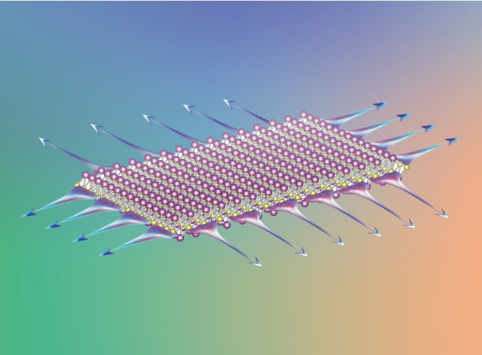
In the study, the researchers used computer simulations to investigate the superconducting behavior of a dimolybdenum nitride (Mo2N) monolayer at different temperatures and with the application of varying strains. The mathematical tool used to resolve the electronic structure of the material was density functional theory (DFT), a simplified model derived from quantum mechanics.
In DFT, used in solid-state physics and theoretical chemistry to resolve many-body systems, the properties of systems with many electrons are determined by means of functionals (functions of functions) — in this case, the spatial distribution of electron density.
“Analysis of electron-phonon coupling enables us to detect the formation of Cooper pairs, which characterize a superconducting state,” Silva said.
A phonon is a mechanical excitation that propagates through the crystal lattice of a solid. In classical physics, it can be described as an elastic wave, but considering that the phenomenon occurs on the atomic scale, it is necessary to use quantum physics, in which case a phonon should be thought of as a quantum of energy that travels through the lattice.
Electron-phonon interaction generates an effective attraction between electrons, which leads to electron pairing, or formation of Cooper pairs. Discovered by Leon Cooper, winner of the 1972 Nobel Prize in Physics, Cooper pairs flow together through the material without energy dissipation, resulting in superconductivity.
“We found that dimolybdenum nitride has a striking property, which is that it’s an electride and at the same time displays superconductivity at relatively high temperatures. Owing to their ionic nature, electrides have pockets of electrons confined in voids in the crystal, whereas superconductors, depending on the temperature, offer no resistance to the flow of electrons. Although these two properties appear to be opposites, they could coexist in the same material. That’s exactly what we showed in our study,” said Zenner Pereira, a professor at the Federal Rural University of the Semi-Arid (Ufersa) in Rio Grande do Norte State, and first author of the Nanoscale article.
An important finding of the study was the strong correlation between the electronic properties of the material and the strain applied. “Our simulations also showed that the Mo2N monolayer became superconductive at the highest temperature of any material in its class at ambient pressure. The transition temperature ranged from 19.3 kelvin to 24.8 kelvin, depending on the strain,” Silva said.
Besides Silva and Pereira, Giovani Faccin, a professor at the Federal University of Greater Dourados (UFGD) in Mato Grosso do Sul, also participated in the study.
About São Paulo Research Foundation (FAPESP)
The São Paulo Research Foundation (FAPESP) is a public institution with the mission of supporting scientific research in all fields of knowledge by awarding scholarships, fellowships and grants to investigators linked with higher education and research institutions in the State of São Paulo, Brazil. FAPESP is aware that the very best research can only be done by working with the best researchers internationally. Therefore, it has established partnerships with funding agencies, higher education, private companies, and research organizations in other countries known for the quality of their research and has been encouraging scientists funded by its grants to further develop their international collaboration. You can learn more about FAPESP at www.fapesp.br/en and visit FAPESP news agency at www.agencia.fapesp.br/en to keep updated with the latest scientific breakthroughs FAPESP helps achieve through its many programs, awards and research centers. You may also subscribe to FAPESP news agency
Recent Posts
- Astronomers detect first direct image of black hole expelling a powerful jet
- WhatsApp rolling out ‘reply with message’ feature within call notifications
- Multi-Device Pairing May Be Arriving for Apple Watch this Year
- Artificial Intelligence Discovers Hidden Giant, a Planet 5 Times Larger Than Jupiter
- Google CEO Sundar Pichai Talks Bard & The Future Of Search
Recent Comments

Astronomers detect first direct image of black hole expelling a powerful jet

Artificial Intelligence Discovers Hidden Giant, a Planet 5 Times Larger Than Jupiter

Scientists explain melting of Antarctic ice sheet dating back 9,000 years

An Unexpected Discovery: Hubble, ESA's Gaia Spot Double Quasar That Existed Over 10 Billion Years Ago

Astronomers detect first direct image of black hole expelling a powerful jet

WhatsApp rolling out ‘reply with message’ feature within call notifications

Multi-Device Pairing May Be Arriving for Apple Watch this Year
